Wednesday, April 6, 2016

Day 13: Op Amp Circuits, Inverting and Non-Inverting Amplifiers, Summing and Difference Amplifiers

In class today we learned about the different types of op amp circuits and what they are usually used for. We learned about a unity gain buffer amplifier, a simple circuit which involves a short circuit connected from the output to the inverting input. The gain of such a circuit is just one (Vout equal Vin); it is usually used to draw more current from a voltage source with high internal resistance.

We then reviewed an inverting amplifier, which involves an op amp circuit with a voltage source connected to the inverting input terminal and a resistor connected across the output and inverting input terminals. The non-inverting input terminal is usually connected to ground. The inverting amplifier amplifies the input signal but also reverses its polarity.

Next, we analyzed non-inverting amplifiers. Their only difference with respect to the inverting amplifier is that the voltage source is applied to non-inverting input terminal instead of the inverting terminal. Non-inverting amplifier are used to amplify output signals without reversing their polarity; they are also used to always make larger signals, since their gain can never be less than or equal to one. If the gain does become one (i.e. by no feedback resistor or an infinite input resistance), the circuit becomes a unity gain buffer amplifier.

We then analyzed a summing amplifier. It is similar to an inverting amplifier, but now consists of voltage sources and resistors in parallel that are connected together to the inverting input terminal. The non-inverting input terminal is connected to ground and there exist a feedback resistor between the output and inverting input terminals. In this circuit the output voltage is the weighted sum of the input voltage. the output voltage is also reverse-polar to the input signal. We then did a lab on summing amplifiers.

Lastly, we spoke about difference amplifiers. They are similar to summing amplifiers but instead the input voltages are subtracted to find the output voltage. A difference amplifier amplifies the difference between two inputs and does not detect any signals shared between the two inputs.


LECTURE:


This problem involved an inverting amplifier with a time-varying input signal (a square wave). The objective was then to find the output time-varying signal. To do so the gain was found, which is just the negative of the quotient between the feedback resistor and the inverting input resistor. Then, knowing that the inverting amplifier amplifies and reverses the polarity of the signal the output signal was found. Looking at the op amp, the negative supplied voltage is zero, which limits the output signal to provide no less than 0 V. The output signal was a square wave with an amplitude of 150 mV centered at +150 mV.


This problem also involved an inverting amplifier. The objective was to find the gain of this circuit and to find the output voltage if the non-inverting input terminal had no voltage source and was just attached to ground.  The gain was found to be -1/2 and the output voltage was found to be -1.64 V. This circuit was solved using nodal analysis.


The relationship between input and output voltage of a non-inverting amplifier was derived above. It was found that the gain is the quotient of the feedback and input resistors added to one. As can be seen, the gain can never be less than 1 since resistances cannot be negative.


Above is the derivation of the relationship between the output voltage and the different applied voltage to the inverting input terminal. As can be seen the output voltage is a weighted sum of the applied voltages to the input,  which is weighted on the feedback resistor and the resistors in parallel to each voltage source applied to the inverting input. As can also bee seen the output voltage in this circuit had a revered polarity compared to the input voltage. This is because the applied voltages are connected in parallel to the inverting input terminal.


In the above problem the input signals across a difference amplifier were provided; the resistors in this amplifier were all assumed to be equal. The objective was to then find the output signal using these two input signals and the assumption of equal resistors. To do so, the difference between the first and second signals was found. In this problem the difference just resulted in the first input signal shifting  down vertically by 1. There is Claptrap giving us a high five for our good work on finding the output signal. He is definitely very interested in this difference amplifier business.


The objective of the above problem was to construct a difference amplifier circuit that would have a gain of 2 and 10 kOhm input resistors. As seen above the circuit was constructed with the specifications. The gain was provided to be 2 by using 20k ohm resistors for the feedback and non-inverting input resistors.


Finally, this circuit was analyzed. It was found that this circuit can be treated as either a difference amplifier or a non-inverting amplifier. Our group was chosen to solve it as a difference amplifier, which allows us to skip over much of the nodal analysis. We found the gain to be 1/3, which reduces the input signal's amplitude from 5 V to 1.67 V. In addition, because the negative voltage of the op amp is connected to ground, the output signal cannot be less than 0 V, which results in a square wave centered at 0.833 with an amplitude of 0.833 V.

LAB:


Summing Amplifiers:

Purpose:

The purpose of this experiment was to design a summing amplifier circuit that would not saturate at any of the input voltages that must be provided to the operational amplifier. The objective was then to choose a gain that would not saturate the op amp in this circuit, which was adjusted via the feedback and input resistors. The circuit was then built and the needed applied voltages were applied to the input, and the output voltages were recorded and tested for accuracy based on the theoretical gain.

Apparatus:


The equipment of this experiment consisted of an OP27 operational amplifier, an analog discovery tool box, a breadboard, a laptop with "Waveforms" software, a DMM, wires and alligator clips. The only really new part of the equipment is the OP27 op amp.

Prelab:


The purpose of this prelab was to design the circuit and modify it to meet its standards before actually building and testing it. A simple summing amplifier was made, with two input voltages at the negative terminal in parallel and the positive input terminal attached to ground. The output voltage as a function of the input voltages and resistances was found for the circuit. Then resistances for the circuit were chosen. It was decided initially that all resistors be the same values of 2.2 kOhms to make the math simpler, as shown in the prelab, but that did not work because the op amp became saturated. +5 V and -5 V sources were applied to the op amp at V+ and V- inputs. Therefore, because of this, the feedback resistor R3 was dropped down to 1 kOhm, but the other two resistors were still left at 2.2 kOhms. This results in a gain of around 0.44, which prevented the op amp from saturating at the input voltages needed.

Procedure:


The difference amplifier circuit was then built and the output voltages were recorded at each input voltages necessary to be applied. The true resistances of each resistor were also measured using an ohmmeter, as seen in the prelab  For the non-inverting terminal, a constant 1 V was applied. For the inverting terminal, voltages of -4 V, -2 V, -1 V, 0 V, 1 V, 2 V, 3 V and 5 V. +5 V and - 5 V were added to the + V and - V terminals. The output voltages were then measured using a voltmeter.


Data Analysis / Conclusion:


As seen above, the output voltages were recorded for each change in input voltage in the inverting terminal. As seen, there was no saturation at any of the applied voltages, which meets that requirement. In addition, the output voltages were inverted polarity-wise, which definitely also meets our requirement and shows that our circuit is set up correctly. Lastly, all of the points for output voltage followed the relationship obtained for the summing amplifier, and, as seen, the gain is roughly 0.44 for each point, which also shows that our circuit was analyzed and built correctly. Overall, our circuit was a success and a summing amplifier that met all of the requirements was created.

Tuesday, March 29, 2016

Day 11: Operational Amplifiers and Inverting Voltage Amplifier

In class today we learned about operational amplifiers and how to analyze electrical circuits in which they are present in. Under the hood an operational amplifier is very complex, with many resistors, capacitors and transistor in an interconnected network. However, we learned that we can simplify them and treat them as a very large resistor attached across the input terminals and a voltage-controlled voltage source in series with a resistor across the output terminal. The dependent voltage source relies on the voltage across the very large resistor. We then learned that we must take into account which input terminal the voltage source is connected to. If it is attached to the non-inverted terminal, we treat the voltage source as positive, and a positive gain should be obtained. If the voltage source is attached to the inverted terminal, the voltage source is treated as negative, and a negative gain is obtained. We also learned about an open loop versus a closed loop. An open loop results in no feedback between the output and input (i.e. the output and input terminals are not connected). A closed loop, as implied, has feedback between the output and input of the op amp (i.e. the input and output terminals are connected.
After, we did the lab titled "Inverting Voltage Amplifier". Once we finished the lab we then learned about ideal operational amplifiers and how so much simpler they make the circuit. An ideal amplifier has an infinite resistance for the resistor connected across the inverted and non-inverted terminals. This means that no current runs through the resistor and therefore no current through the wires attached to the terminals. No current means no voltage across the resistor; this results in the voltage-controlled voltage source providing no voltage, and therefore means no current running through the output wire of the amplifier. 

LECTURE:


This problem involved an operational amplifier with the voltage source attached to the noninverted terminal. The operational amplifier was redrawn to consist of a resistor attached to the terminals with a potentional difference Vd and on another branch a voltage source dependent on Vd with a resistor in series. The output voltage was found via node-voltage analysis, and the gain of the amplifier was also calculated. 


This problem involved an operational amplifier as well. However, the voltage source was attached to the inverted terminal, resulting in a positive output voltage. Node-voltage analysis was then used again to solve for the output voltage, the gain of the amplifier and the current running through the wire running outside of the output terminal. Again, as with all operational amplifiers, the voltage controlled voltage source is dependent on the potential across the resistor connected to the inverted and non-inverted terminals.


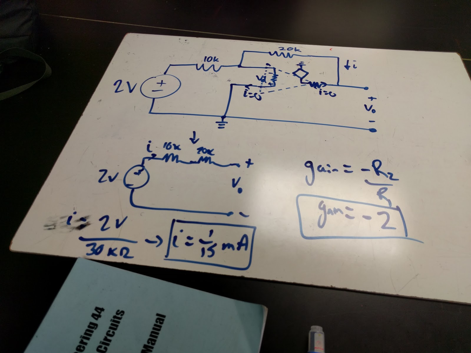
In this problem, the operational amplifier was treated as ideal. This really simplifies the circuit greatly; in this problem it became a simple voltage source and two resistors in series with each other and the voltage source. The current through the 20 kOhm resistor was then found, along with the gain of the amplifier.

LAB:

Inverting Voltage Amplifier:

Purpose:

The objective of this experiment was to test the gain of the operational amplifier experimentally by seeing the output voltage change when the input voltage was changed. The saturation points for the operational amplifier were also found. Because the voltage is connected to the inverted terminal, it is expected that the gain will be negative.

Prelab:


In this prelab the resistance of resistor R2 was found, and the relationship between the output and input voltages (i.e. the gain) was also found in terms of the resistors. The gain was mathematically found to be -2.

Apparatus:


The equipment used in this experiment consisted of the following pieces: an OP27 operational amplifier, an analog discovery toolbox, a laptop with Waveforms software, resistors, a breadboard, a digital multimeter, wires and alligator clips.

Procedure:


The schematic of the circuit seen in the prelab above was created, as shown in the above picture. The circuit is zoomed in to show more detail, as seen below:


In this circuit, the + 5 V and - 5 V sources (provided by the red and white wires, respectively) were attached to terminals 7 and 4 of the operational amplifier, respectively. The two resistors R1 and R2 were both attached to the second terminal on the op amp, which is the inverted input voltage terminal. In addition, the other end of resistor R2 was connected to terminal 6, or the output terminal. The waveform source (yellow wire) was attached to the end of resistor R1 to provide the varying voltages needed. A ground wire was then attached to terminal 3 of the op amp. Lastly, the DMM, acting as a voltmeter, was connected to terminal 6 in parallel with the resistor R2. The other end of the voltmeter was also attached to another ground wire. An ohmmeter was then used to measure the true resistances of the resistor, whose values are shown below:

Data Analysis:


The waveform generator was then used to apply input voltages ranging from -3 V to 4 V to the circuit, in increments of 0.5 V. The output voltages were then measured using the voltmeter and recorded. The data is seen above in the table of output vs input voltages. At -2.5 V and -3 V the op amp reached its upper saturation, and at 2 V and above it reached its lower saturation point. This data was then used to make a graph that represents the model of the op amp used. This graph is shown below:


Conclusion:

The graph obtained was the expected graph, because there were saturation points on both ends of the voltage spectrum. In addition, as seen by the data, when the input voltages were negative the output voltages were positive and vice versa. This shows that the gain of the op amp is negative, which is expected since the voltage source is attached to the inverted terminal. In addition, the output voltage was nearly the negative of the double of the input voltage at each point, with the exception of saturation points; this shows that our gain is -2. This was the calculated and expected gain, which shows that the simplification used for these operational amplifiers is true and correct. Lastly, looking back at the graph, the slope is -2; this shows that the slope is the gain value and that the relationship determined between the output and input voltages via the resistors used (and therefore gain) is accurate.

Friday, March 25, 2016

Day 9: Maximum Power Transfer Theorem and Resistance Measurement

In class we learned about maximum power transfer theorem, which allows us to find the maximum power that a circuit could deliver to a resistor based on thevenin voltage and resistance. In order for a resistor to draw the most power it could out of a circuit, its resistance must equal the thevenin resistance, which was derived in class by taking the partial derivative and setting equal to zero the equation for power as a function of the load resistance. The equation is found below:

From the derivative with respect to load resistance, it was found that thevenin resistance must equal load resistance. Plugging in thevenin resistance for load resistance, we obtain:


Then, we did a problem involving finding max power in a variable resistor. A problem was also done involving applying these concepts to a robotics application to find the internal resistance in a battery. In addition another problem finding the load resistance for max  power in that resistor was done.

We then did a lab on Maximum Power Transfer, which is explained in more detail in the lab section. Lastly, we learned about source modeling and how engineers take into account internal resistance for sources so that the source provides the expected current or voltage. We also did an example on this application. In addition, we learned about a Wheatstone bridge circuit and how it can be used to measure internal resistance via a galvanometer; an example involving this application was performed along with a review problem that puts all of today's concepts together.

LECTURE:


This is the derivation to find the load resistance needed to obtain the maximum power in that resistor. It was done by taking the derivative with respect to the load resistance and setting it to zero since at max power the slope is zero. Again, it was found that the load resistance must equal the Thevenin resistance.


In this problem the Thevenin equivalents were found along with the current through the circuit if the load resistance was 8 ohms. Then, the resistance needed for max power was found (12 ohms) and the power at that resistance was calculated (33.33 W). In addition, power values at different load resistances was found to give us an idea of the curve for power as a function of load resistance.


This problem is the robotics application of max power. The motors in parallel were treated as resistors, and the Thevenin resistance was found. The max power was then found, and using the value that energy needed and amphours used to run this robot was found.


In this simpler problem the load resistance needed to obtain max power was found, which was just using the addition of resistors to find the Thevenin resistance.


In the problem above, the voltage provided to the load resistor was found using source modeling. The above problem shows that a practical source does not actually provide the expected voltage in every circuit it is applied to; it only approaches its expected source values, but only when the load resistance is high enough. If not, it actually provides a lower source value depending on the resistance of the load resistor, as shown above.


In this problem, the resistance needed for R_s in the wheatstone bridge so that no current goes through the galvanometer was found (50 ohms). This type of circuit is used to measure resistance more accurately for medium levels.


Lastly, this problem was just review of the maximum power transfer theorem, along with Thevenin equivalents and source transformations.


LAB:

Maximum Power Transfer:

Purpose:

The purpose of this experiment was to test the max power transfer theorem by setting up a simple circuit with a 5V voltage source, a source resistor of 4.7 kOhms and a variable resistor all in series. The variable resistor was adjusted at resistance values of 1 kOhm to 10 kOhms with an  interval of 1 kOhm, and the power through the resistor at those resistances was found by first measuring the voltage. (NOTE: This lab was performed different than what the lab manual contains; we were proving the maximum power theorem instead of just showing that its conjugate (source resistance equal load resistance) is false).

Apparatus:


The apparatus in this experiment consisted of an analog discovery (5 V source), a source resistor (4.7 kOhm), a potentiometer, a breadboard, a laptop with Waveforms software, a digital multimeter, alligator clips and wires.

Procedure:

The schematic of the circuit in the apparatus section was built as shown below:


The voltages across the potentiometer for each resistance value were then measured with a voltmeter. The resistance in the potentiometer was measured with an ohmmeter. The voltages were then used to calculate the power at each resistance, and the graph below was made using Logger Pro.


The above data was used to make the graph of power versus load resistance below. A model fit was then manually made using the equation for power, which was seen in the introduction.


Data Analysis:

Looking at the graph, it peaks at about 4700 ohms, which is the resistance of our source resistor. This confirms the maximum power theorem, which states that max power is obtained when the load resistance is equal to the source resistance. The equation for the model fit is shown more closely below:


Looking at the equation, A is our thevenin voltage squared, which is 25 volts squared. In the graph, it is in millivolts squared (25000). In addition, B is the source resistance, which is 4700 ohms. The correlation obtained is perfectly 1, which shows our model is an excellent representation of  the maximum power transfer theorem.


Friday, March 18, 2016

3/17/16 Day 8: Every Circuit Practice, Thevenin's Theorem and Norton Equivalents

LECTURE:

We first did more practice using Every Circuit by building the circuit below in the application and finding the current across the 6 ohm resistor.


We then learned about Thevenin's Theorem, which allows us to simplify any linear circuit across a load (usually a resistor) to a voltage source and resistor in series. This voltage source is called the Thevenin voltage and the resistor is called the Thevenin resistance. The Thevenin resistance is obtained by setting all independent current and independent voltage sources to zero (i.e. voltage sources become wires and current sources become open circuits). The resistors left in the circuit are then added to find the equivalent resistance, which turns out to become the Thevenin resistance.

To find the Thevenin voltage, the different techniques learned, such as node voltage method, mesh current method, superposition and source transformations can be used to find the voltage across the load of interest. The load is also removed from the circuit while measuring both the Thevenin voltage and resistance. 

The schematic of the circuit above was then applied to Thevenin's Theorem to find the current across the 6 ohm resistor. This is seen below:


The Thevenin voltage was found to be 30 V and the Thevenin resistance was found to be 4 ohms. In the new circuit, the Thevenin voltage source, the Thevenin resistor and the load resistor are in series. Dividing the Thevenin voltage by the equivalent resistance (4 + 6 = 10 ohms) it can be seen that the current across the 6 ohm resistor was also found to be 3 A using Thevenin equivalents.

In another problem, the same objective as the previous problem, to find the current across the load resistor, was achieved by using Thevenin's Theorem. In this case, the current as a function of the resistance  value of the load resistor was obtained. It was found that the Thevenin resistance was 10 ohms and the Thevenin voltage was 40 V. Redrawing the Thevenin circuit, we get the 40 V Thevenin power supply connected to the 10 ohm Thevenin resistance and the load resistor.


Doing so we get the function of the current across the load resistor as a function of the resistance to be the Thevenin voltage divided by the equivalent resistance, or:

Then, the problem asked us to solve for the current running through the load resistor when it has various resistance values. This is done by just substituting the value into R_L in the current equation and simplifying.

We were then supposed to learn about Norton's Theorem, which is, simply putting, the idea of using source transformations in Thevenin equivalents. However, we were barely able to scratch the surface of Norton's Theorem due to an unexpected emergency drill performed by Mt. SAC in our building.

LAB:

Thevenin's Theorem:

Purpose:

The purpose of this experiment was to determine experimentally the validity of Thevenin's Theorem in linear circuits. This was achieved by taking a provided circuit, finding the Thevenin equivalents of voltage and resistance across a load resistor R, then measuring the load voltage across R in the original circuit and the created Thevenin equivalents circuit and comparing the two values, which ideally should be nearly equal if Thevenin's Theorem holds to be true.

In addition, the power dissipated in the load resistor R as a function of load resistance was found by using a potentiometer, which is a variable resistor. The voltages at different resistances was obtained, and a graph was created using that data.

Prelab:

The circuit in the above schematic was the circuit used in this experiment. As seen, the circuit was first created in Every Circuit for extra practice, and to determine the voltage across the load resistor (which was given a value of 6.8k ohms) to compare with the measured load voltage for validity; the load resistor is the highest resistor in the circuit, in series with the 1k ohm and 1.5k ohm resistors. The load voltage was found to be 0.22 V.

Then, the Thevenin voltage and resistance were calculated as seen below:


The Thevenin resistance was found by turning off all voltage sources and finding the equivalent resistance in the circuit. It was found to be 7.4k ohms. Next, the Thevenin voltage was found by finding the voltages across the 4.7k ohm and 6.8k ohm resistors, then subtracting the two to find the voltage difference across points a and b. The Thevenin voltage was found using mesh current analysis, and was found to be 0.455 V. 

Apparatus:

Most of the equipment used in this lab was just the usual equipment used in all circuits labs, and consisted of different resistors, an analog discovery power supply, a breadboard, a laptop with Waveforms software, alligator clips, a DMM and wires. The only unique apparatus used in this experiment was a potentiometer, or a variable resistor. This was used in determining the power as a function of load resistance.

Procedure:

First, the actual resistances of the used resistors was measured using an ohmmeter. Then. the circuit provided in the Every Circuit schematic was built without including the load resistor. The open-circuit voltage across the 1.5k ohm and 1k ohm terminals was then measured using a voltmeter, as seen below:


The Thevenin voltage was measured as 0.448 V. In addition, the Thevenin resistance was also measured by replacing the voltage sources with wires, then connecting the ohmmeter across the terminals a and b (one end of th1 1k ohm and 1.5k ohm resistors), as seen below:


The Thevenin resistance was measured to be 7.36k ohms. Then, a random load resistor with a resistance value between 4k ohs and 10k ohms was integrated into the circuit. A 6.8k ohm resistor was used, just because in Every Circuit a 6.8k ohm resistor was placed as the load resistor. The circuit is shown in the picture below:


The load voltage was measured as 0.212 V. After, the Thevenin equivalent circuit was built, which consisted of a 0.455 V source in series with a bunch of resistors that added to an equivalence of 7.4k ohms.  The load resistor used in the previous circuit was then integrated into the Thevenin equivalent circuit, and the voltage across the load resistor R was measured, as seen below:


Thevenin circuit sketch

The load voltage in the Thevenin circuit was measured to be 0.209 V, which is lower than expected due to the higher Thevenin resistance of 7.59k ohms. Lastly, the load resistor was replaced with a potentiometer in the original circuit. Its resistance was changed constantly so that the load voltage could be measured as a function of the load resistance. These data points were then used to find the power of the potentiometer as a function of the load resistance, using the formula for the power of a resistor due to voltage, or P = (V*V)/R. The setup is found below:


Data Analysis and Conclusion:


Seen above is all of the data measured in this experiment, such as resistance values, load voltages, Thevenin voltages and Thevenin resistances.

The Thevenin resistance was measured to be 7.36k ohms, which is very close to the theoretical of 7.4k ohms (a percent error of -0.54%). The open circuit voltage was also measured to be 0.448 V, which is also very close to the theoretical value of 0.455 V (a percent error of -1.54%). 

The voltage across the load resistor was found to be 0.212 V. Based on the Every Circuit schematic the true voltage was found to be 0.22 V, which is close to the measured value (a percent error of -3.64%). 

The voltage across the load resistor in the Thevenin equivalent circuit was found to be 0.209 V, which is still fairly close to the expected value of 0.22 V (a percent difference of -5.0%). The reason it is a little off is due to the higher resistance in the Thevenin circuit. 

Below is the data of resistance versus voltage for the potentiometer measurements.


As the resistance increased, the voltage decreased, which is expected. Below is the data for the power versus resistance for the potentiometer and the graph which shows the equation of this relationship.


The maximum power theorem states that the max power in the load resistor is reached when its resistance is equal to that of the Thevenin resistance. Therefore, it was found that the max power drawn by the load resistor occurs when it is 7.4 kOhms, and the max power is:

It seems that our data is significantly off. This is due to the potentiometer being hard to integrate into the circuit and to measure the exact resistance. The difficult of using the potentiometer is what threw off our data. If actual resistors were used our data would become much more accurate; it was just difficult to predict so when we never learned about the maximum power transfer theorem prior to this experiment.

Summary:

In class we first learned about Thevenin's theorem. We then did more practice in Every Circuit and used Thevenin's Theorem in two problems. After, we did the Thevenin's Theorem lab and created a Thevenin equivalent circuit. Lastly, we scratched the surface of Norton's Theorem and learned that we will learn more about it next class along with the maximum power theorem.