Sunday, May 15, 2016

Day 24 5/12/16: Impedance and Admittance, KCL and KVL in Frequency Domains and Equivalent Impedance

We first learned more about impedance, which is the equivalent of resistance for alternating current. We learned that impedance has both a real and imaginary part, with the real portion being the resistance of the resistor and imaginary portion being the reactance of the the capacitor and inductor. The reactance of an inductor is jwl and that of a capacitor is 1/jwC. We also learned that at very high frequencies, an inductor acts like an open circuit and a capacitor acts like a short circuit. We also learned about admittance, which is the inverse of impedance. It contains a real portion, which is the conductance, and an imaginary part, which is called susceptance. The sum of the conductance and susceptance is the inverse of the sum of resistance and reactance. We then did two problems involving finding current and voltage using impedances.

After these two problems, we did a lab titled "Impedance", which is explained in more detail in the "LAB" section below. We then reviewed Kirchhoff's laws in circuits with alternating current, which are used exactly the same as in dc current. KVL and KCL were found to hold for phasors as well.

We then learned about impedance combinations. It was found that impedances in series add, and the equivalent impedance in parallel is 1 over the sum of the inverse of the individual impedances. We then did a problem involving finding the equivalent impedance.

Lastly, the concept of phase shifters was gone over slightly. A problem was then done using phase shifters.


LECTURE:

Above is shown the magnitude of the impedance and the angle formed by the phasor as functions of resistance and reactance. This is found using polar coordinates.


The objective of the above problem is to find the current in the circuit and to find the voltage across the capacitor. First, the impedance of the circuit was found, and the current was obtained by dividing the voltage by the impedance of the circuit. The voltage of the capacitor was then obtained by multiplying the current by the impedance of the capacitor alone.


In the above problem, the objective was to find the voltage across the capacitor. This was done by multiplying the current by the impedance of the capacitor.


The objective is to find the equivalent impedance of this circuit. The impedance of the capacitor and resistor were added, and then the equivalent impednance was found by inversing the sum of the inverse of the impedance of the inductor and the previous impedance combination found.


In this problem, the voltage across the inductor was the objective to determine. First, the equivalent impedance for the inductor and capacitor was determined. Then, a voltage divider was used to find the voltage across this equivalent impedance. Because the capacitor and inductor are in parallel, it is know that the voltage across both is equal.


In this derivation, the phase shift and gain for a specific case when the resistor is equal to the reactance of a capacitor in an RC circuit was found. The phase shift was determined to be -45 degrees and the gain 0.5 of the input voltage. 


LAB:

Purpose:

The purpose of this experiment is to determine the impedance of a resistor, inductor and capacitor experimentally. Another purpose is to determine the gain of each component experimentally and the phase shifts between the current.

Prelab:


In the prelab, the theoretical current through the circuit, the voltage across the circuit elements under analysis (resistor, capacitor, inductor), the gain as a result of each element and the phase shift were determined. Above is the calculations for the resistor and the inductor. The calculations for the capacitor are shown below:


All of this data was then summarized in the table below:


As a correction, the phase shift for the inductor should be 90 degrees instead of 82.4, and the phase shift for the capacitor should be -90 degrees instead of -7.9.


Apparatus:

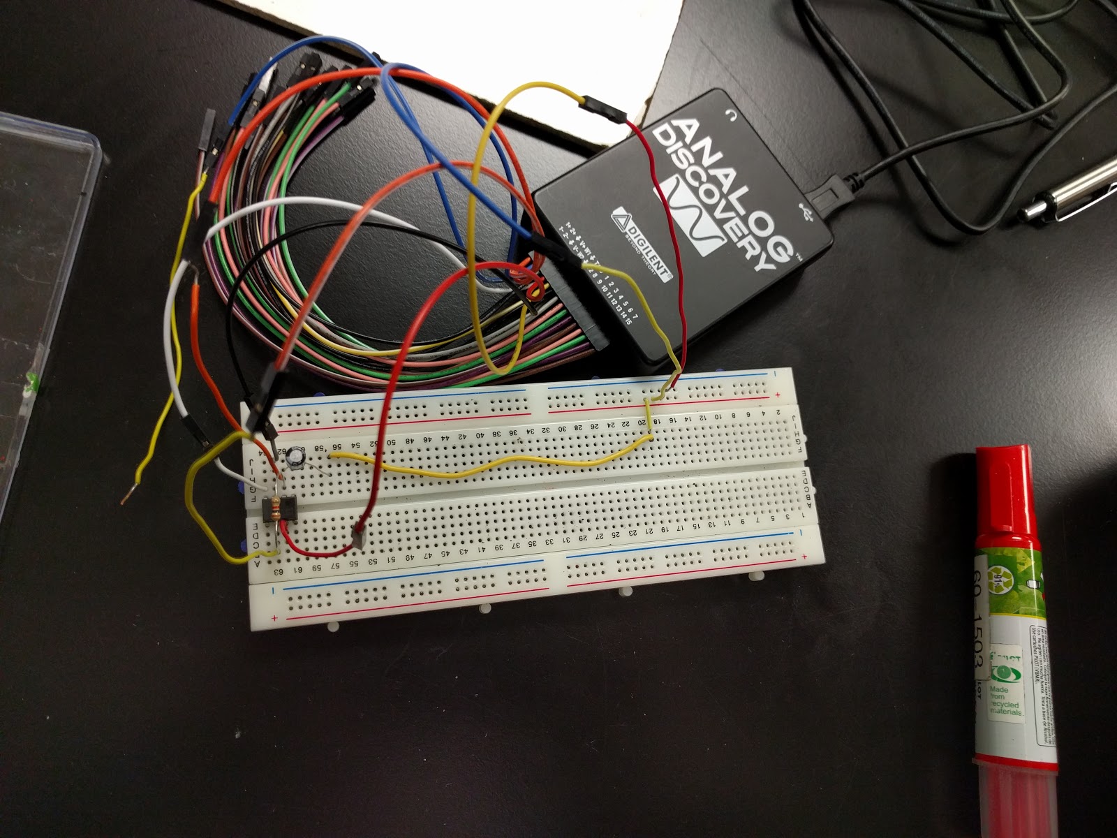
The equipment of this experiment consists of a breadboard, an analog discovery, resistors, a capacitor, an inductor, wires and a laptop with waveforms software.

Procedure:


First, all of the above schematics consisting of  RL, RC and resistor circuits shown above were built on one breadboard. Then, using the circuit with resistors only, a sinusoidal input with an amplitude of 2 V and an offset of 0 V was applied. This voltage input was applied at frequencies of 1 kHz, 5 kHz, and 10 kHz. The oscilloscope channel 1 was then used to measure the current through the circuit by measuring the voltage across the 47 ohm "internal" resistor then dividing that value by its resistance. The voltage across the resistor under analysis was measured using channel 2 of the oscilloscope. An image of the oscilloscope for the resistor circuit is shown below:


Using the oscilloscope window, the current through the circuit, the gain and the phase shift were determined, which is shown in the data section. The same procedure was done three times for this circuit, with each time at a different frequency.

The same procedure seen above was performed for the inductor at all three different frequencies as well. The oscilloscope for the inductor is shown below:


Again, the same procedure was done for the capacitor verbatim. The oscilloscope window for the capacitor is shown below:


Data:


Above is the data obtained from the oscilloscope window for the resistor circuit. The same data was measured at all of the three different applied frequencies of 1 kHz, 5 kHz and 10 kHz. This data includes the current function, the voltage function across the resistor under analysis, the experimental gain of the circuit and the phase shift between the voltage of the circuit element and current.

Below is the same data at the same frequencies for the inductor and capacitor, respectively..

Inductor

Capacitor

Analysis/Conclusion:

Analyzing the data of the resistor circuit, the current measured through the circuit for each trial (13.39 mA, 13.65 mA, and 13.4 mA for the 1 kHz, 5 kHz and 10 kHz) is very similar to the theoretical (13.6 mA), which shows that the analysis and set up were correct. The slight deviations are due to uncertainties in the values of the circuit elements. Because the currents are similar, the voltages are also similar. The experimental gains obtained (0.695 for 1 kHz, 5 kHz and 0.68 for the 10 kHz) are also very similar to the theoretical gain of 0.68, which is expected. Again, the deviations are due to uncertainties in the element values and error in measuring values in the oscilloscope. Lastly, the phase shift for both values is 0, which is expected for a resistor.

Analyzing the data for the inductor, the experimental current for 1 kHz (40.5 mA) is similar to the theoretical (42.2 mA), and the difference is due to human uncertainty when obtaining values from the oscilloscope and uncertainty in the values of the circuit elements. It was found that the current and voltage varies depending on the frequency, which is expected because the voltage and current are related and time-dependent by v = Ldi/dt. Because the voltage differs depending on the frequency, the gain also differs. However, for the 1 kHz, the obtained gain (0.127) is close to the theoretical gain of 0.133.  Lastly, the experimental phase shift (88.2 degrees) is also close to the theoretical (90 degrees).

Analyzing the data for the capacitor, the voltage, current and gain also differ depending on the frequency, because they are time-dependent and related by i = Cdv/dt. However, analyzing at 1 kHz frequency, the experimental current (4.7 mA) is deviating from the theoretical (5.8 mA). It is unknown exactly why, but it is thought that it could be due to a large uncertainty in the capacitance, since the experimental gain and theoretical gain turned out to be exactly the same (0.99). In addition, the experimental phase shift is also exactly equal to the theoretical (-90 degrees).


Above is the experimental and theoretical impedances for each circuit element under the different applied frequencies, along with the percent differences between these frequencies. The percent differences are large for some of the capacitor values and for the inductor values because of uncertainty in the element values. Because the elements we were working with are small, any small change results in a big difference in impedance.

Wednesday, May 11, 2016

Day 23 5/10/16: Sinusoids, Phasors and Complex Numbers

All we did in class was lecture on sinusoids, phasors and complex algebra. No labs were done in class this day. We reviewed what sinusoid signals were, which are signals that have the form of a sine of a cosine function. Graphing the sinusoidal signal when given the function, and determining the function when given the graph were reviewed and practiced in a problem. We then reviewed how to switch from sine to cosine functions and vice versa using a phase angle. Polar coordinates were then reviewed and derived, and determining the resultant of two signals using polar coordinates was reviewed and practiced in a problem. Next, phasors were reviewed, which could be written in complex numbers and Euler's identity. Converting from complex numbers to phasor notation and back was also reviewed, and adding/ subtracting/ multiplying/ dividing phasors was reviewed. It was found that adding and subtracting phasors is more efficient using complex numbers, and multiplying / dividing is easier in phasor notation. Two problems applying these concepts were then performed. Another problem adding signals in phasors was also solved. Then, phasor relationships were applied to circuit elements, such as resistors, capacitors and inductors. For resistors, Ohm's law is used to convert voltage signals to time-varying current across the resistor. The voltage and current of a resistor are in phase. For a capacitor, the voltage lags the current by 90 degrees, and the current can be determined using i = c(dv/dt). Using this, the impedance of a capacitor was found to be -j/wC, and the voltage of a capacitor is the impedance of a capacitor times the current. The impedance of a capacitor is imaginary, which means realistically it does not have any impedance. Lastly, for an inductor, the voltage is L(di/dt), and using this, the impedance was found to be jwL. Again, the impedance of a capacitor is imaginary.

LECTURE:


In the above problem, phase shifts and vertical shifts for trig functions were explored, along with the base knowledge of determining an equation for a trig function by analyzing its graph. The first voltage time-varying signal was a sinusoidal wave that has an amplitude of 0.17 V and a vertical shift of 0.03 V. The function also had a period of 0.012 s.

The second voltage function was the same voltage function as the first, with the exception that the sine function is shifted a tenth of a period to the right. Therefore, for a phase shift to the right, the magnitude of the shift must be subtracted from time.


In this example, two voltage signals were added together using phasors. The angle between them was found to be 30 degrees, and the amplitude was determined by using the law of cosines.


The derivation for polar coordinated was solved for in the above picture. The relationships between x, y, r and phi were determined in these derivations.


This example involved adding sinusoidal signals together in phasor notation. First, in order to add the two signals, they were converted to complex numbers from phasor notation. Once the resultant in complex notation was found, the amplitude and the angle were determined using polar coordinates. These values were then used to determine the resultant signal in phasor notation. Then, the inverse of the phasor was determined by using Euler's identity. The inverse could have also been determined if the identity for the inverse of phasor notation was known. The inverse of a phasor is one over the amplitude and negative of the original angle.


In the above picture, a couple of different sinusoidal time-varying signals were re-written in phasor notation. In order to write a sinusoidal signal in phasor notation, it must be first converted into a positive cosine function by including a phase shift of + or - 90 degrees.


In this example, Euler's identity and a complex number were converted to a sinusoidal form. First, the Euler's identity was converted to complex number form, and then the radius and angle were determined from the complex form. These values were then used to determine the cosine function of the phasor. For the complex number, the radius and angle were first determined, and these values were used to find the cosine function of the phasor.


In this problem, the above two voltage signals were added by converting to complex number notation. Then, the radius and angle were determined of the resultant, which were used to find the resultant voltage signal in the trig form.


Thursday, May 5, 2016

Day 22 5/5/16: Series and Parallel RLC Circuits with Sources and Second order Op Amp Circuits

In class today we first learned a little about how wireless charging works; it really involves the induction of current in one coil by another. Inductive mode involved the transmitter working at a value slightly different than the resonant frequency, causing max power. It is achieved by having two inductors of equal diameter lined up closely together so that their separation is much smaller than the diameter. The other mode is resonance mode, in which the receiver works at resonant frequency. The seperation between these two coils is much larger.

We then reviewed step response of a series RLC circuit with a forced response (i.e. voltage source) connected. It turns out that the same exact concepts and formulas are used when just looking at a source free RLC circuit, with the addition of adding the forced response to the formulas. Next, we did a problem involving a voltage source in a series RLC circuit. We then reviewed step response of a parallel RLC circuit with a forced response (i.e current source). Again, it turns out that all the concepts and equations of a parallel source free RLC circuit hold true, with the exception that the forced response must be added to the equations. After, we did a problem involving a current source connected to a parallel RLC circuit. The two previously learned concepts that are helpful in the analysis of these circuits is that the capacitor resists voltage change and inductor resists current change. Therefore, at time zero the capacitor acts as a short circuit and the inductor as an open circuit. At time infinity (steady state) the capacitor is fully charged and acts like an open circuit; the inductor then acts like a short circuit.

After lecture, we did a lab titled "RLC Circuit Response". After the lab, we then learned about second order op amp circuits. As expected, nodal analysis is used in these circuits, and the op amps do not affect much the solution of the RLC circuit (i.e. they are solved very similarly to RLC circuits without op amps). The only time op amps are taken into account in these circuits is simply the initial values to find constants. In addition, the neper and natural frequencies of a second order op amp circuit are not the same as that of a series or parallel RLC circuit, and they are derived by using KCL and nodal analysis. The solutions to the differential equations though are the same as those for op-amp free RLC circuits.


LECTURE:


This problem involved a series RLC circuit with a voltage source. The objective was to find the current as a function of time in this circuit after the resistor and voltage source are short-circuited. This involved finding the neper and natural frequencies and from those values determining whether the circuit is underdamped, critically damped or overdamped. The rest of the problem is seen below.


The initial values for the circuit were then used to determine the constants of the current function.


This problem involved a current source connected to a parallel RLC circuit. Again, the objective was to find the current through the inductor as a function of time. This required to find the neper and natural frequencies and from there determining the damping of the circuit. The rest of the problem is found in the picture below.


The initial values for current across the inductor were then used to find the constants of the current function. 

LAB:

RLC Circuit Response:

Purpose:

The purpose of this experiment is to test the second order differential equation governing a series RLC circuit with a voltage source by finding theoretical values and comparing to measured values. The step response will also be tested and compared to the expected behavior, and data from the response will be compared to theoretical values.

Pre-lab:


 In the prelab of this experiment, the neper and natural frequencies of the second order RLC circuit being tested were obtained. Based on these values, it was found that the circuit is underdamped since the neper frequency is less than the natural. The damping ratio was then obtained, along with the values for the characteristic roots of the differential equation and the differential equation of this circuit itself.

Apparatus:


The equipment of this experiment consisted of the usual; an analog discovery, a breadboard, resistors, a capacitor, an inductor, a computer with Waveforms, wires, alligator clips and a DMM.

Procedure:


First, the circuit seen in the schematic in the prelab was constructed. In addition, the wavegen wire (yellow) was used to provide a square wave at 200 Hz with an amplitude of 1 V and an offset of 1 V. This allows providing to the circuit a voltage of 2 V while allowing it to enter its step response by turning off the applied voltage. Channel 1 was used to keep track of the input voltage in the oscilloscope window, and channel 2 was used to measure the voltage across the resistor in the RLC circuit (not the one used to impede the voltage source) and display it in the oscilloscope window.

Then, the square wave was applied to the circuit and the output voltage of the resistor was measured in the oscilloscope window. The window is shown in the data section. From the step response in the window, the experimental values of natural frequency, damping ratio, and characteristic roots were determined. This data is also shown in the data section of this blog.

Data:


As can be seen from the window above, which contains the input voltage and the voltage across the resistor as a function of time, the step response takes the form of an underdamped circuit, which is expected since the circuit was found to be underdamped in the prelab. N addition, based on the graph, the average voltage across the resistor was found to be about 40 mV when the 2 V is supplied, which is close to the expected value of 45.7 mV from using voltage divider. Using the step response, the natural frequency along with the damping ratio and other experimental values in this series RLC circuit were determined, and are shown below:


The percent error between the damping ratios was also calculated.

Data Analysis / Conclusion:

The experimental natural frequency from the obtained step response was found to be 1.28 x 10^4 rad/s, which is reasonably far from the theoretical value of 1.00 x 10^4 rad/s (a 28.0 % percent error). The discrepancy is most likely due to either the capacitance of the capacitor being off by the assumed value, or uncertainty in the inductance of the inductor. Because the inductance of the inductor cannot be measured and the resistance of the resistor was too small to be measured accurately, the same value of neper frequency was assumed, which in reality does skew our experimental values even further. The experimental damping ratio was then determined, which was found to be 0.0431, which is considerably off from the expected value of 0.0550. The percent error, as seen above, was calculated to be -21.7 %, which is a reasonably large value. Again, this is due to making many assumptions that are in reality not true; these assumptions were only made because the equipment needed to measure the real values was not available to us. These assumptions are the resistance of the resistor, the capacitance of the capacitor, the inductance of the inductor and therefore the same neper frequency. Because the neper frequency is dependent on the very small value of resistance used, any uncertainty in the resistance changes the true neper frequency drastically, and therefore changes the damping ratio even more. 

5/3/16: Day 21- Series and Parallel RLC Circuits

We first reviewed finding boundary values for second order circuits, which will help us greatly in analyzing RLC circuits and their components. We reviewed that a capacitor resists sudden changes in voltage and inductors resist sudden changes in current, which will help us find the voltages and/or currents in these RLC circuits at time 0. We also reviewed that at time equals infinity the inductor acts as a short circuit and the capacitor acts as a open circuit under steady state conditions.We then did a problem involving these concepts in a series RLC circuits to find voltages and currents at t = 0 and t -> infinity.

We then analyzed source free RLC circuits with all components in series. KVL was used to determine the second order differential equation of this circuit. One possible solution to this differential was used (i = Ae^st) to determine its validity, but it turned out that it didn't quite possibly explain all aspects of the circuit. It was still plugged back into the equation to find the two natural frequencies "s", or the roots of the obtained quadratic. Using these frequencies the neper frequency alpha (R/2L) and the undamped frequency omega (1/(LC)^-1/2) were found. Because there were two values of s obtained and the initial predicted solution did not explain all of the aspects, it was found that the solution contains two components A1 and A2. It was then determined that when alpha is greater than omega, the circuit is overdamped; when they are equal, it is critically damped; and when alpha is less than omega, it is underdamped. We then learned about the different current solutions used for those three cases and their respective graphs. We then did a problem involving calculating the roots and figuring out if the circuit is overdamped, underdamped, or critically damped. A lab titled "Series RLC Circuit Step Response" was then performed.

We then went over parallel RLC circuits that were source free. These circuits are very similar, with the exception that KCL was used to find the second order differential equation. In addition the DEQ of a parallel RLC circuit relates voltages whereas the DEQ of a series circuit related currents. In addition, alpha of a parallel circuit is now 1/2RC and not R/2L. Everything else stays the same, including equations for different damped cases and the other formulas. We then did a problem applying these concepts to a parallel RLC circuit.


LECTURE:


In this problem, the circuit involved an inductor in series with a voltage source and a capacitor parallel to the 2 ohm resistor. At DC conditions the inductor acts as a wire and the capacitor acts as an open switch. Then, using KVL the current was obtained in the above simplification of the circuit and the voltage across the 2 ohm resistor was calculated.


In this problem, the objective is to determine the second order differential equation governing the series RLC circuit. It was found that the differential equation can be dependent on charge or current. di/dt at time zero was found using the equation for voltage of an inductor. Then, using the value for di/dt at time zero and the second order DEQ the initial voltage was determined.


In this derivation the second order DEQ of the series RLC circuit with respect to current was determined. Then, a plausible solution for current involving an exponential function was plugged into the DEQ and simplified in terms of the solution.


The previous derivation was continued even further, and the solutions for the value s were obtained using a quadratic equation since the obtained formula for the plausible solution was a quadratic. Then, the solutions were written in terms of alpha (the neper frequency) and the angular frequency (omega). The neper frequency for the series RLC circuit is R/2L and the angular frequency is (LC)^(-1/2).


The objective of the problem seen above is to find the two constants "s" of the above RLC circuit and whether the circuit is underdamped, critically damped or overdamped. It was found that the circuit is overdamped since its neper frequency is greater than the angular frequency. Then, knowing that the solutions to the values of s is -alpha +/- (alpha^2-omega^2)^(1/2), the values were calculated.


In this problem, the equation for output voltage as a function of input voltage was obtained for the series RLC circuit. Then, the circuit was determined to be overdamped because the neper frequency is larger than the angular frequency. The damping ratio was then obtained, which is just alpha over omega and termed by the Greek letter zeta. As expected, zeta hould be higher than one since the circuit is overdamped. Finally, the two values of the constant s was calculated.


In this problem, a parallel RLC circuit was analyzed, and the damped status and voltage functions were determined, as seen above. The two values of the constant s were also determined. It was found to be overdamped, and the constants in the voltage function were found by using v(0) and dv(0)/dt. The rest of the problem is seen below.


LAB:

Series RLC Circuit Step Response:

Purpose:

The purpose of this experiment was to model and test a series RLC circuit. The step response was determined and tested by comparing the measured values of natural and neper frequencies to the expected. Another purpose of the experiment was to design a critically damped RLC circuit without changing the natural frequency. The step response was then remeasured and compared t theoretical values.

Prelab:


In this prelab, the second order differential equation of the series circuit was used to find the output voltage (voltage across the capacitor) in terms of the input voltage. Then, the natural frequency, damping ratio and damping frequency were determined, along with the type of damping the circuit is. Then, the two values of the constant s were determined.

Apparatus:

The equipment of the experiment consisted of the usual equipment, such as an analog discovery toolkit, a breadboard, a laptop with Waveforms, resistors, an inductor, a capacitor, a DMM, alligator clips and wires.

Procedure:


First, the circuit schematic seen in the prelab was built. A 1 ohm resistor, a 1 mH inductor and a 4.7 uF capacitor were used. Then, a 1 V square step input voltage with an offset of 1 V (alternates between 2 V and 0 V) at a frequency of 100 Hz was applied using the wave generator function. Channel 1 was used to measure the input voltage and Channel 2 was used to measure the voltage across the capacitor. The voltages were then measured using the oscilloscope window. The graph f the voltages is pasted in the data section.

Then, the natural frequencies, damping ratio and period were estimated from the oscilloscope window.


Next, the circuit was modified to obtain a critically damped circuit without changing the natural frequency of the circuit. This was done by changing the resistance and keeping the inductance and capacitance the same, since the angular frequency is dependent on inductance and capacitance. The new circuit consisted of a 29.5 ohm resistor and the same inductance (1 mH) and capacitance (4.7 uF), all in series, exactly like the underdamped circuit. Then, the same procedure was used for the underdamped circuit, as seen above. The oscilloscope window containing the voltage graphs is pasted in the data section.

Data:


The above picture of the oscilloscope window is the graphs of the input voltage and output voltage for the underdamped circuit. The step response is the quickly decaying oscillation seen at the changes in voltage. This step response is shown closer in the diagram below.


The calculated natural frequency and damping frequency are posted in the data analysis section. The above step response is expected because it indicates an underdamped system, which is the type of circuit used in this experiment.


The above picture is the oscilloscope window / step response for the critically damped circuit. Practically the circuit is slightly overdamped since it was difficult to accurately obtain the needed resistance of 29.2 ohms. This step response is also expected because it correlates for the most part with a critically damped system, which is what we have. The two voltages never meet, which is correlating to a critically damped circuit. 

Data Analysis / Conclusion:


The above picture is the calculated data for the underdamped circuit from the step response of the oscilloscope window. The angular frequency was found to be  1.5 x 10^4 rad/s, which is very close to our theoretical value of 1.46 x 10^4 rad/s. In addition, the damped ratio was found to be 0.0533, which is slightly off from 0.0343. This is mostly due to the resistance actually being 1.6 ohms and not 1 ohm, changing the neper frequency significantly. Because of this and due to being the value being super small, any small change causes a large difference.

The neper frequency is found to be 800 rad/s from the data, which is also far off from the expected of 500 due to, again, the large uncertainty in the resistance. Therefore, the damped frequency was found to be 14978 rad/s, which is  close to the theoretical value of 14578 rad/s. This is because the value is so large, so any change will not affect it much. 

Lastly, the values of s were calculated from the data to be -800 +/- 14978i, where the theoretical vaues were -500 +/- 14578i, which the difference again is due to alpha being large because of the large uncertainty in the resistance.

Tuesday, April 26, 2016

4/26/16 Day 19: First Order Op Amp Circuits (Integrators and Differentiators)

In class today we first quickly reviewed the basic concepts of capacitors and inductors, such as storing energy and preventing sudden changes in voltages (for capacitors) or current (for inductors). We then learned about placing RC and op amp circuits together, termed first order op amp circuits. We learned about two very common RC op amp circuits, termed the integrator and differentiator. The integrator consists of a capacitor connected from the output to the input (a feedback). Using differential equations it was found that the output voltage in an integrator depends on the integral of the input voltage with respect to time; the gain of this circuit was found to be the negative of the reciprocal of the time constant of an RC circuit (tau = RC). We then analyzed a practical integrator and the output voltage depending on the signals applied to the input terminal.

After, we learned about differentiators, which are RC op amp circuits that have a capacitor connected to the input. These circuits differentiate the input signals to determine the output voltage. The gain in these circuits are negative of the time constant for an RC circuit (tau = RC).

Next, we reviewed switching functions from mathematics because they are very useful in engineering when analyzing RC and RL circuits and when trying to cause these circuits to operate by switching. Switching functions are functions that have a discontinuity or have a discontinuous derivative; they very well model the opening or closing of a switch in these first order circuits. We learned about the three most common switch functions, termed the unit step, the unit impulse, and the unit ramp. A unit step is zero for all values of t less than zero and one for all values of t greater than zero. The unit step is discontinuous at t = 0 (undefined). The unit step can also be shifted horizontally depending on at what time is considered "zero" (i.e. the frame of reference per se). We then did a lab titled "Inverting Differentiator" after learning about the unit step function.

After the lab, we went back to switching functions. Another one we learned is the unit impulse function, which is 0 at every value of t except zero. At t equals zero, it is undefined. This function is also known as the delta function. It has an area of 1, and the area can be modified simply by  multiplying the delta function to a scalar. For example, 10 times delta has an area of 10. The delta function can also be horizontally shifted like any other function. In addition the delta function, when multiplied to another function, provides only the value of the instantaneous point at t equals zero or t naught if shifted horizontally.

Lastly, another useful switching function is the unit ramp function, which is obtained by integrating the unit step function. The unit ramp function is zero for t less than zero and is a function of time for t greater than 0. Originally, it is a linear graph of slope 1 and y intercept of 0 at t greater than 0. Like any other function, the unit ramp function can also be horizontally shifted. After learning about these two switch functions, a problem involving voltage sources acting as switch functions in a circuit was solved.

We then applied the unit step function in an RC circuit, where the unit step was provided by an external source like a voltage source. The voltage as a function of time was determined for such a circuit using KCL and separable differential equations. It was found that v = Vs+(Vo-Vs)e^(-t/RC) for t greater than zero, and simply Vo for t less than zero (since the unit step is zero before t equal zero). Using i = C dv/dt the current is Vs/R*e^(-t/RC). The forced response of a step response of an RC circuit is Vs, and the natural response is the rest ((Vo-Vs)e^(-t/RC)). The total response can also be written in the same way, where Vs = V (infinity) and Vo = V(0). An example involving this idea was then performed.

Finally, the step response of an RL circuit was analyzed. It is very similar to the step response of an RC circuit, with the exception that now the voltage function in an RC circuit is the current function in an RL circuit. For an RL circuit, i(t) = Is+(Io-Is)e^(-Lt/R). The voltage is then given by v = L*di/dt. A problem using this idea was then solved. We then went over delay circuits slightly, which are RC circuits and a lamp in parallel to the resistor.

LECTURE:


Above is the derivation for the output voltage of an integrator as a function of the input voltage. As can be seen, the circuit is not called an integrator for no plausible reason; this circuit integrates the input voltage with a gain of -1/RC, or -1/tau, where tau is the time constant of an RC circuit.


In this problem, a square wave, triangular wave, and sinusoidal wave signals were inputted to a practical integrator (which is an ideal integrator but a large resistor in parallel with the capacitor). The resistor parallel to the capacitor is used to dissipate energy, or the result would be the op amp saturating. As seen in the sinusoidal input wave, the output would be a cosine wave with amplitude 1/RC times the original amplitude. Looking at the square wave input signal, the output wave signal is a triangular wave that should actually begin towards the negative amplitude (our signs were switched by accident on the y axis). Again, the amplitude is still the original times 1/RC. Lastly, looking at the triangular input wave, the resulting output wave would be a sawtooth-like wave that consists of half- parabolas arcing up and down. Again, the wave would go towards the negative amplitude first due to the negative gain, which is not shown in our graph due to switching the signs on the y axis. The amplitude is still the same A/RC. All of these output wave graphs were determined by integrating the input functions and multiplying by the gain for an integrator (-1/RC).


The above picture is a schematic of the circuit implemented in the previous analysis. The gain of this RC op amp circuit was found to be -10.


In this problem, the voltage of the capacitor as a function of time using switch functions was provided, and the objective was to find the current across the capacitor. Using the fundamental law for capacitors (i = c dv/dt), the current was obtained. The derivative of the unit step was found to be delta and the derivative of the unit ramp was found to be the unit step. The graphs of voltage and current were then drawn using the voltage and current functions.


In the above derivation, the current across the capacitor in an RC circuit with a step response was derived.


In this example, the voltage across the capacitor as a function of time in this step response RC circuit was determined by finding the voltage at infinity, at zero, and the time constant. The voltage function was then written using those determined values. The current was then obtained using the current law for a capacitor.


This problem involves the step response of an RL circuit. It was solved similarly to the previous problem, with the exception of the current being found first and the voltage later. The current at infinity, at zero, and the time constant were obtained to write the current equation. The voltage was then obtained using the voltage law for an inductor.
LAB:

Inverting Differentiator:

Purpose:

The purpose of this experiment was to experimentally analyze a differentiator circuit to compare with the expected behavior in order to determine the validity of the relationship derived between the output and input voltages for a differentiator. 

Prelab:


The output voltage as a function of the input voltage for the differentiator was determined in the pre-lab, where the gain was dependent on the resistor and capacitor. Using this relationship the output voltage as a result of an actual applied input wave function was determined, where the input voltage was a sinusoidal function of amplitude A and frequency w/(2pi). 

In addition, in order to obtain a gain of 1, the appropriate resistor to use in the differentiator was determined.

Apparatus:


The apparatus of this experiment consisted of an OP27 op amp, a 1 uF capacitor, an analog discovery, a resistor, a breadboard, a laptop with Waveforms, wires, alligator clips and a DMM. 

Procedure:


To begin, the inverting differentiator circuit was actually built; its schematic is found in the pre-lab. It was decided to use a 1 kOhm resistor to reduce the gain so that the op amp does not saturate during the experiment. The +5 V and -5 V inputs from the analog were used in the op amp at its +V and - V ends, respectively. A Wavegen input wire was then used as the input voltage to this circuit. The non-inverting input was simply attached to ground. The oscilloscope was then used to measure input and output voltages; the input voltage was measured using channel 2 and the output voltage was measured using channel 1. The output voltage is seen across the resistor, so the channel inputs were placed across the resistor. For channel 2, only one input was used and it was connected adjacent to the wavegen input, since if two inputs were used the oscilloscope would measure no voltage due to being no potential difference across the inputs. The actual resistance value of the 1kOhm resistor was measured using a DMM and was found.

Then, using the Waveforms application, sinusoidal functions of varying frequencies were inputted to the op amp. All the sinusoidal functions had an amplitude of 100 mV and an offset of zero. The first sinusoidal wave had a frequency of 1 kHz. The oscilloscope was then used to measure the output voltage, and prior to this the expected amplitude of the output voltage was calculated (the reasoning is seen in the pre-lab). The phase shift was also determined to be pi/2, since the derivative of sine is cosine, and they are shifted apart by 90 degrees. The oscilloscope window of this sinusoidal wave is shown below:


The same was performed for a sinusoidal wave input with frequency of 2 kHz. Again, the expected amplitude was also calculated prior.


Lastly, the same procedure was performed for a sinusoidal input wave of 500 Hz. The window is shown below.


For all of these screenshots of the oscilloscope window, the blue wave us the input voltage and the yellow wave is the output voltage.

Data:

The expected voltage amplitude, the measured voltage amplitude (determined from the oscilloscope window) and the percent difference between the two was tabulated for each sinusoidal wave of varying frequency, and is shown below:


This table also includes the measured resistance of the 1 kOhm resistor used as well as the input and output voltage functions determined by using the law for a differentiator op amp circuit.

Data Analysis / Conclusion:

As can be seen in the table, the expected values and the measured values for each sinusoidal wave of varying frequency were very similar, which proves the validity of the relationship between the input and output voltages for a differentiator. The small percent difference between each is mostly just due to the uncertainty in reading of the amplitude from the oscilloscope windows. Any other small errors are just due to unaccounted resistance or the sensitivity of the op amp to the input signals.

Looking at the shapes of the input and output signal functions, the input is a sine function of amplitude 1 V. The output signal is also a sinusoidal wave, but it is actually a cosine wave, determined by the pi/2 phase shift from the input signal. The pi/2 phase shift is seen because when one signal is at a peak of a trough, the other signal is at zero, and vice versa. It is expected that the output signal would be a cosine wave from the law of a differentiator; the output is related to the derivative of the input.